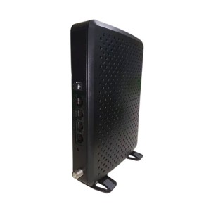
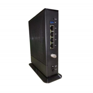
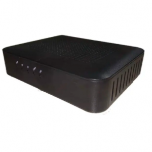
ECMM, DOCSIS 3.0, 1xGE, MCX/SMB/MMCX, DV110IE
Short Description:
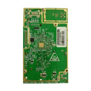
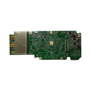
The MoreLink’s DV110IE is a DOCSIS 3.0 ECMM Module (Embedded Cable Modem Module) supporting up to 8 downstream and 4 upstream bonded channels to deliver a powerful high-speed Internet experience.
The DV110IE is temperature hardened for integration in other products that are required to operate in the outdoor or extreme temperature environment.
Product Detail
Product Tags
Product Detail
The MoreLink’s DV110IE is a DOCSIS 3.0 ECMM Module (Embedded Cable Modem Module) supporting up to 8 downstream and 4 upstream bonded channels to deliver a powerful high-speed Internet experience.
The DV110IE is temperature hardened for integration in other products that are required to operate in the outdoor or extreme temperature environment.
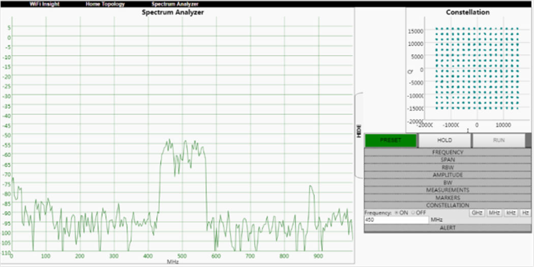
Base on Full Band Capture (FBC) function, DV110IE is not only a Cable Modem, but also can be used as a Spectrum Analyzer.
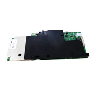
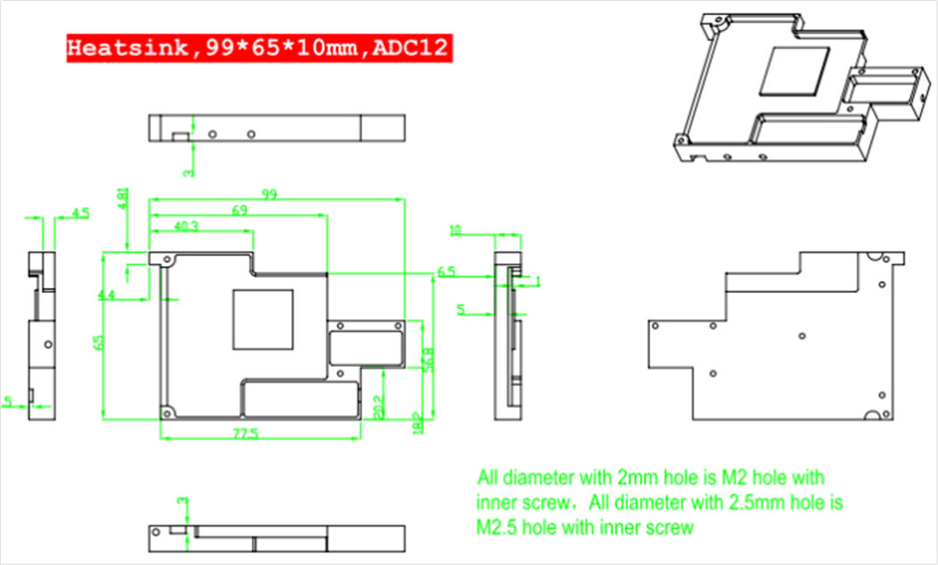
Heatsink is mandatory and application specific. Three PCB holes are provided around the CPU, so that a heatsinking bracket or similar device can be affixed to the PCB, to transfer the generated heat away from the CPU and towards the housing and environment.
This product specification covers DOCSIS® and EuroDOCSIS® 3.0 versions of the Embedded Cable Modem Module series of products. Throughput this document, it will be referred as DV110IE.
Product Features
➢ DOCSIS / EuroDOCSIS 3.0 compliant
➢ 8 downstream x 4 upstream bonded channels
➢ Temperature hardened
➢ Support Full Band Capture
➢ RF Connector: SMB for combined DS and US
➢ RF Connector: MMCX for separate DS and US
➢ SPI, UART, GPIO signals are accessible by Signal Interface
➢ One Gigabit Ethernet Port supporting auto-negotiation
➢ Standalone External Watchdog (Optional)
➢ Temperature sensor on board (Optional)
➢ Accurate RF power level (+/-1dB) at all temperature range
➢ Embedded Spectrum Analyzer
➢ DOCSIS MIBs, SCTE HMS MIBs supported
➢ Open system API and data structure for 3rd party application access
➢ Software upgrade by HFC network
➢ Small Package Size of PCBA\
The DV110IE is a core module having a very small foot print and easily integrated in other HFC products. The system block as below:
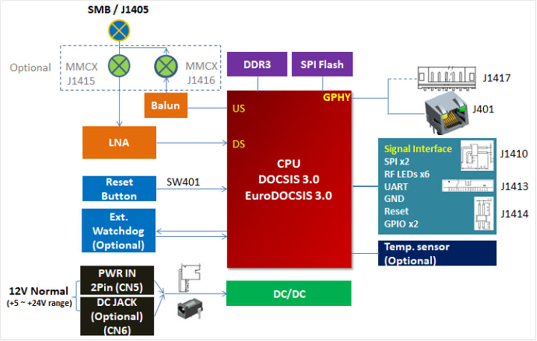
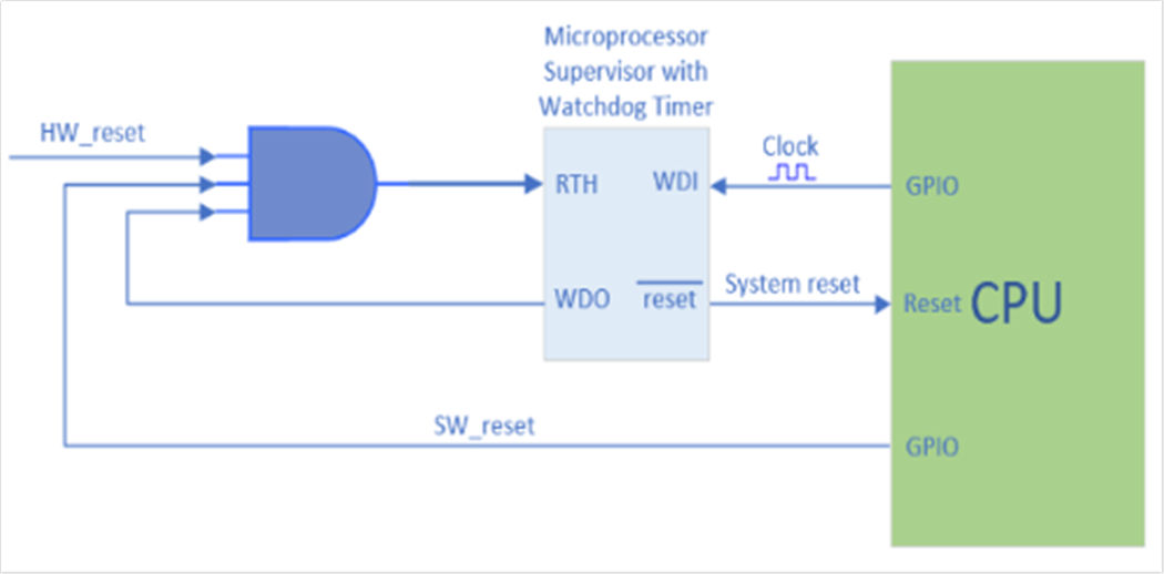
External Watchdog
An external watchdog is used to make sure the system’s operation reliably. Watchdog is kicked by the Firmware every once in a while so that the CM does not reset. If there’s something wrong with the CM Firmware, then after a certain period (watchdog time), the CM will reset automatically.
Application
➢ Transponder, such as Power Supply, Fiber Node, UPS, CATV Power
➢ IP-Camera Video
➢ Digital Signage
➢ Wi-Fi Hotspot Traffic
➢ Emergency broadcast
➢ 4G LTE and 5G Small Cell
➢ DVB-C or Hybrid STB embedded CM
➢ Smart City Applications
➢ CATV/QAM/DOCSIS/HFC Instruments and Apparatuses
Support HMS MIBs
|
1 |
SCTE 36(HMS028R6) | SCTE-ROOT and scteHmsTree definition |
|
2 |
SCTE 37(HMS072R5) | scteHmsTree subgroups |
|
3 |
SCTE 38-1(HMS026R12) | propertyIdent objects |
|
4 |
SCTE 38-2(HMS023R13) | alarmsIdent objects |
|
5 |
SCTE 38-3(HMS024R13) | commonAdminGroup objects and the commonPhyAddress object |
|
6 |
SCTE 38-4(HMS027R12) | psIdent objects |
|
7 |
SCTE 38-5(HMS025R13) | fnIdent objects |
|
8 |
SCTE 38-7(HMS050R5) | transponderInterfaceBusIdent objects |
|
9 |
SCTE 38-10(HMS115) | RF Amplifier MIB objects |
|
10 |
SCTE 25-1 | Hybrid Fiber Coax Outside Plant Status Monitoring |
Spectrum Analyzer: Main Features
- Scan frequency range (5 – 1002 MHz)
- RBW setting
- Marker (When Locked, Power Level/ QAM/ post BER / pre BER/ Symbol Rate)
- Constellation
- Peak/ Average
- Alert
- Unit (dBm/ dBmV/ dBuV)
- Nosie level <-50 dBmV for DS
- Noise level <-20 dBmV for US
Technical Parameters
|
Protocol Support |
||
| DOCSIS/EuroDOCSIS 1.1/2.0/3.0 SNMP v1/v2/v3 TR069 |
||
|
Connectivity |
||
| RF | x1 SMB Connector for combined D/S and U/S (J1405) x2 MMCX Connectors for separate D/S (J1415) and U/S (J1416) |
|
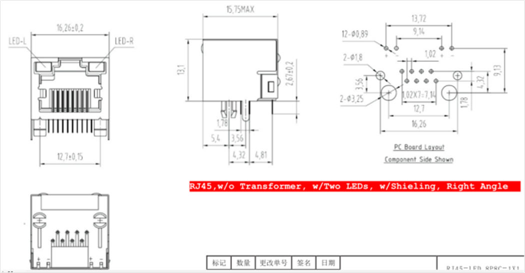
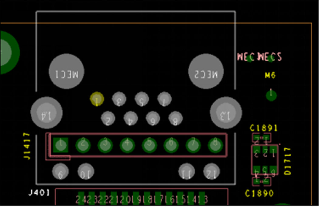
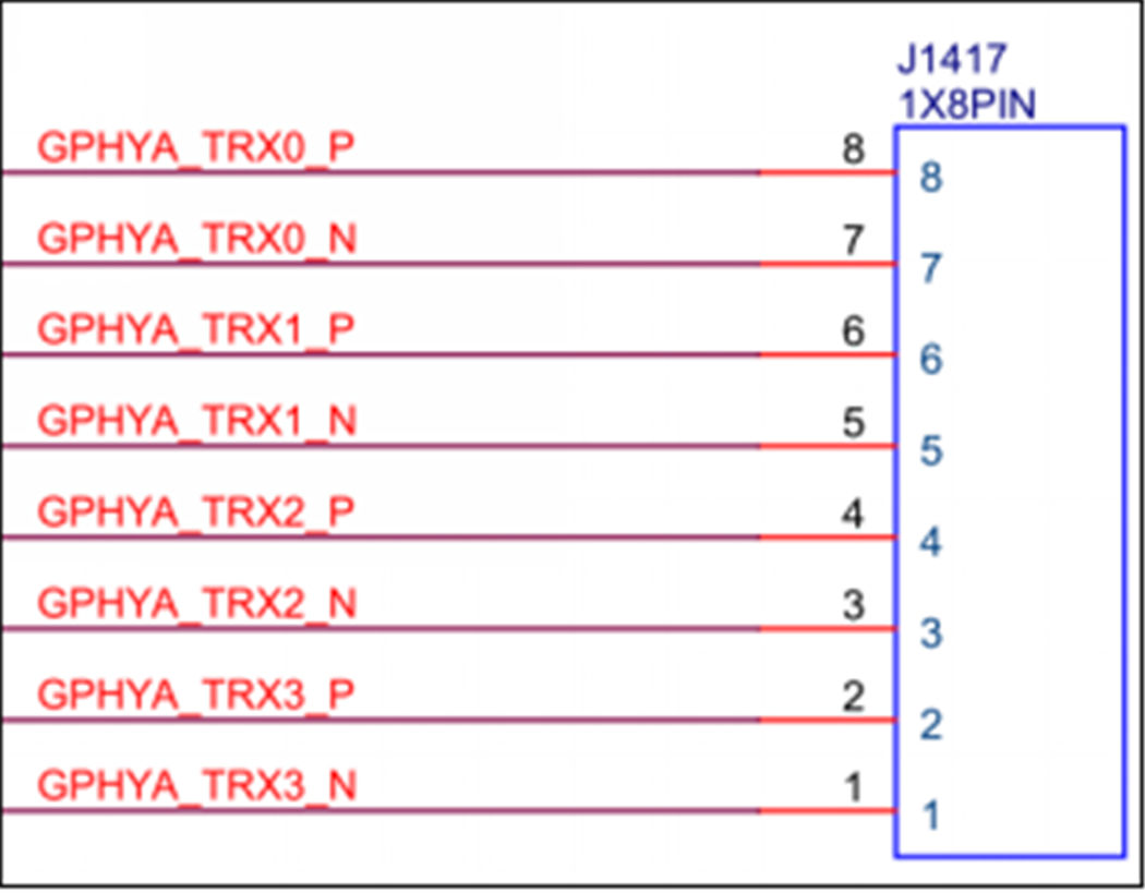
| RJ45 | 1x RJ45 Ethernet port 10/100/1000 Mbps (J401) | |
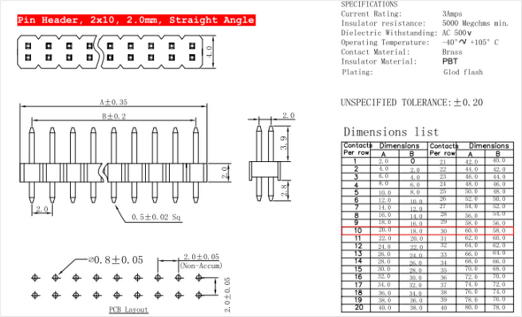
| Signal Interface | Pin Header, 2x10, 2.0mm, Right Angle (Option) (J1410) Box Header, 2x10, 2.0mm, Straight Angle (Option) (J1413) Pin Header, 2x10, 2.0mm, Straight Angle, Male (J1414) Pin Definitions see Table #1 |
|
|
RF Downstream |
||
| Frequency (edge-to-edge) | 88~1002 MHz (DOCSIS) 108~1002MHz (EuroDOCSIS) |
|
| Channel Bandwidth | 6MHz (DOCSIS) 8MHz (EuroDOCSIS) 6/8MHz (Auto Detection, Hybrid Mode) |
|
| Modulation | 64QAM, 256QAM | |
| Data Rate | Up to 400Mbps by 8 Channel bonding | |
| Signal Level | Docsis: -15 to +15dBmV Euro Docsis: -17 to +13dBmV (64QAM); -13 to +17dBmV (256QAM) |
|
|
RF Upstream
|
||
| Frequency Range | 5~42MHz (DOCSIS) 5~65MHz (EuroDOCSIS) 5~85MHz (Optional) |
|
| Modulation | TDMA: QPSK,8QAM,16QAM,32QAM,64QAM S-CDMA: QPSK,8QAM,16QAM,32QAM,64QAM,128QAM |
|
| Data Rate | Up to 108Mbps by 4 Channel Bonding | |
| RF Output Level | TDMA (32/64 QAM): +17 ~ +57dBmV TDMA (8/16 QAM): +17 ~ +58dBmV TDMA (QPSK): +17 ~ +61dBmV S-CDMA: +17 ~ +56dBmV |
|
|
Networking |
||
| Network protocol | IP/TCP/UDP/ARP/ICMP/DHCP/TFTP/SNMP/HTTP/TR069/VPN (L2 and L3) | |
| Routing | DNS / DHCP server / RIP I and II | |
| Internet Sharing | NAT / NAPT / DHCP server / DNS | |
| SNMP version | SNMP v1/v2/v3 | |
| DHCP server | Built-in DHCP server to distribute IP address to CPE by CM’s Ethernet port | |
| DCHP client | CM automatically gets IP and DNS server address from MSO DHCP server | |
|
Mechanical |
||
| Status LED | x6 (PWR, DS, US, Online, LAN, RF Levels) | |
| Factory Reset Button | x1 (SW401) | |
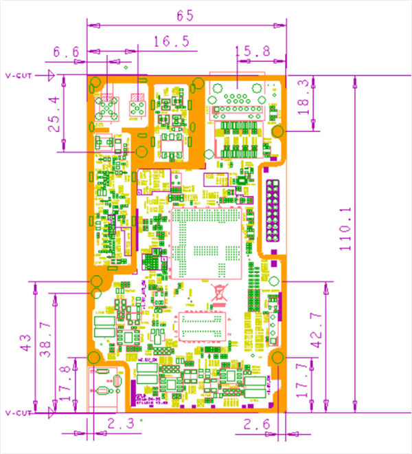
| Dimensions | 65mm (W) x 110mm (H) x 17mm (D) | |
|
Environmental |
||
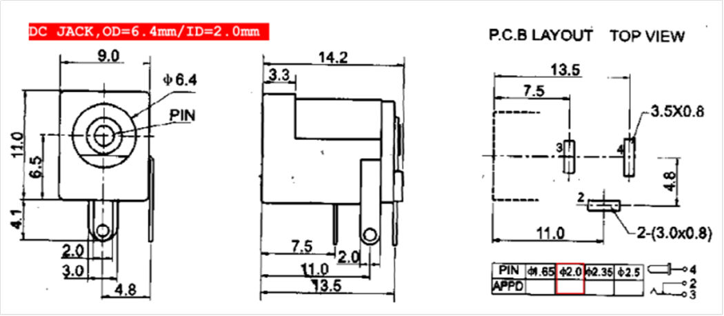
| Power Input | DC Jack (6.4mm/2.0mm) (CN6) Wafer Header, 1x 2, 2.0mm, Right Angle. (Option) (CN5) Support wide power input: +5VDC ~ +24VDC |
|
| Power Consumption | 12W (Max.) 7W (TYP.) | |
| Operating Temperature | Commercial: 0 ~ +70 oC Industrial: -40 ~ +85 oC |
|
| Operating Humidity | 10~90% (Non Condensing) | |
| Storage Temperature | -40 ~ +85 oC | |
Signal Interface: Pin Definition (J1410, J1413, J1414)
| Port Pin | Signal Description | Signal Type | Signal Level |
|
1 |
SPI MOSI | Digital Output | 0 to 3.3VDC |
|
2 |
SPI CLOCK | Digital Output | 0 to 3.3VDC |
|
3 |
SPI MISO | Digital Input | 0 to 3.3VDC |
|
4 |
DS LED (lit when low) | Digital Output | 0 to 3.3VDC |
|
5 |
Ground | Reference | 0V |
|
6 |
ONLINE LED (lit when low) | Digital Output | 0 to 3.3VDC |
|
7 |
US LED (lit when low) | Digital Output | 0 to 3.3VDC |
|
8 |
PWR LED (lit when low) | Digital Output | 0 to 3.3VDC |
|
9 |
SPI Chip Select 1 | Digital Output | 0 to 3.3VDC |
|
10 |
SPI Chip Select 2 | Digital Output | 0 to 3.3VDC |
|
11 |
GPIO_01 | Future use | 0 to 3.3VDC |
|
12 |
Ground | Reference | 0V |
|
13 |
Ground | Reference | 0V |
|
14 |
Serial port transmit enable | Digital Output | 0 to 3.3VDC |
|
15 |
Reset (Active low) | Digital Input | 0 to “Open” or 3.3VDC |
|
16 |
RF LEVEL Green LED (lit when low) | Digital Output | 0 to 3.3VDC |
|
17 |
GPIO_02 | Future use | 0 to 3.3VDC |
|
18 |
RF LEVEL Red LED (lit when low) | Digital Output | 0 to 3.3VDC |
|
19 |
UART Transmit | Digital Output | 0 to 3.3VDC |
|
20 |
UART Receive | Digital Output | 0 to 3.3VDC |
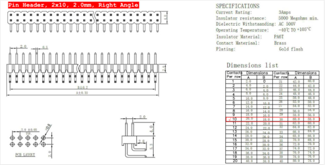
J1410: Pin Header, 2x10, 2.0mm, Right Angle.
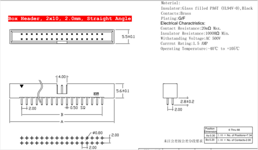
J1413: Box Header, 2x10, 2.0mm, Straight Angle.
J1414: Pin Header, 2x10, 2.0mm, Straight Angle.
J401: RJ45, w/o Transformer, w/Two LEDs, w/Shielding, Right Angle
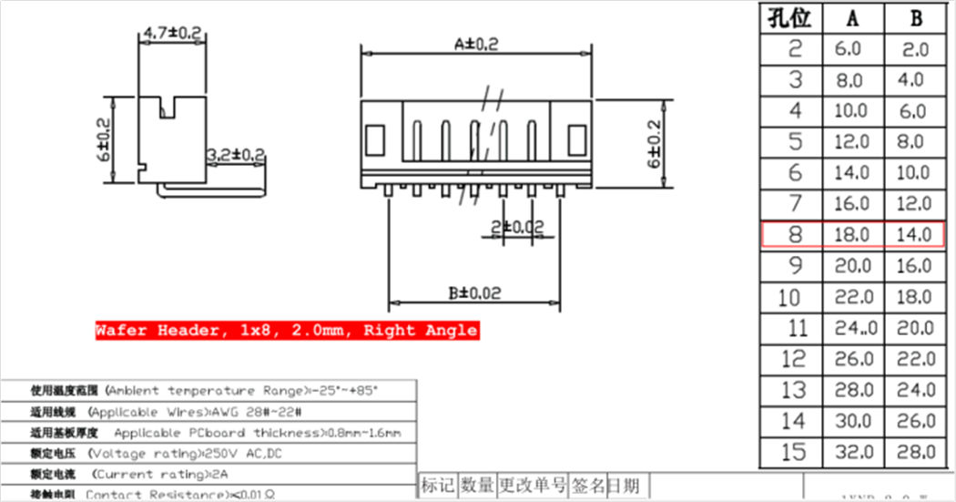
J1417: Wafer Header, 1x8, 2.0mm, Right Angle.
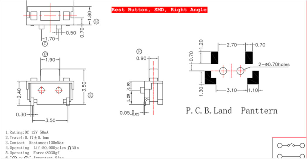
SW401: Reset Button, SMD, Right Angle.
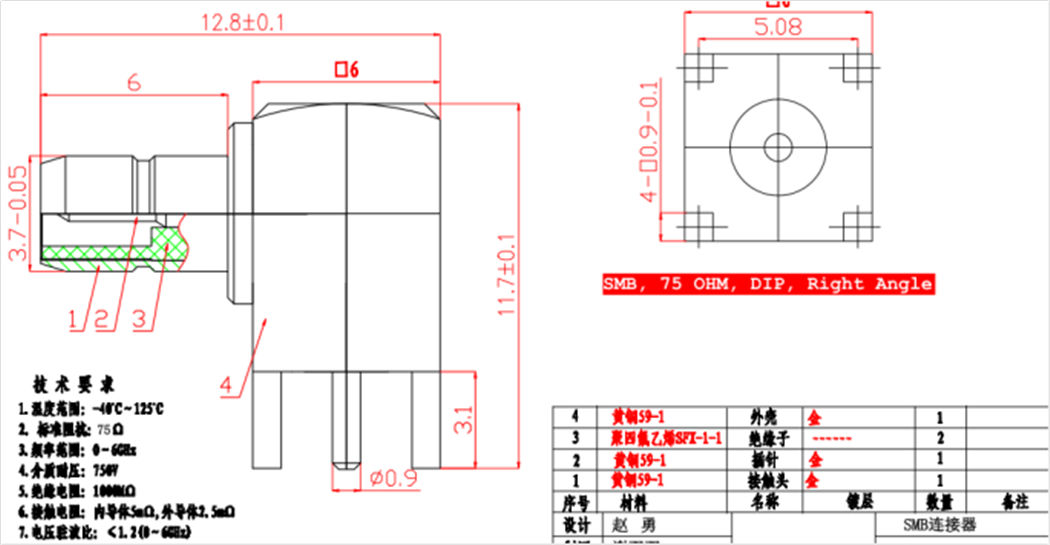
J1405: SMB, 75 OHM, DIP, Right Angle. Combined D/S and U/S RF Signal.
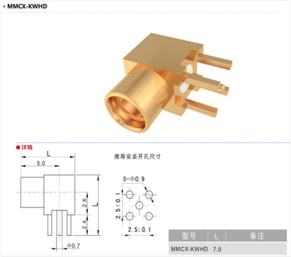
J1415, J1416: MMCX, 50 OHM, DIP, Right Angle. Separate D/S and U/S RF Signal.
CN5: Wafer Header, 1x 2, 2.0mm, Right Angle. Populate at the bottom side of PCB.
Pin1 - VIN
Pin2 – GND

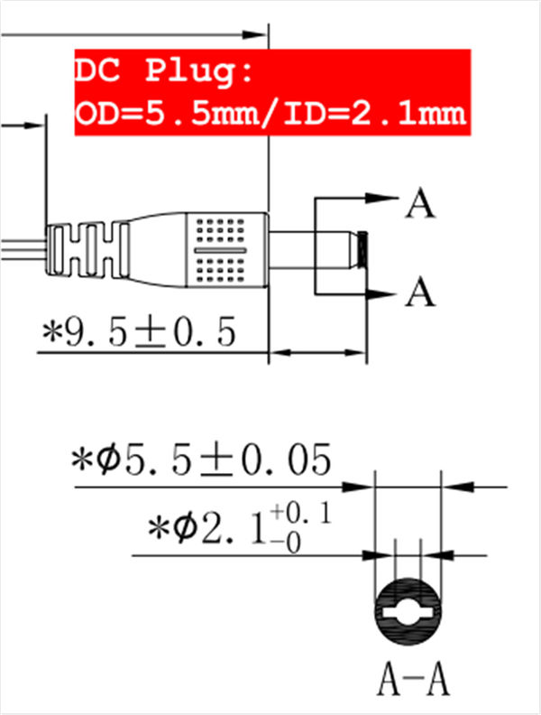
CN6: DC JACK, OD=6.4mm/ID=2.0mm. Matching DC Plug OD=5.5mm/ID=2.1mm
Heatsink Dimensions (Unit: mm)
PCBA Dimensions (Unit: mm)
